
近期更新 立即订阅
Optimizing Semiconductor Yield with High-Precision Thermoforming Systems
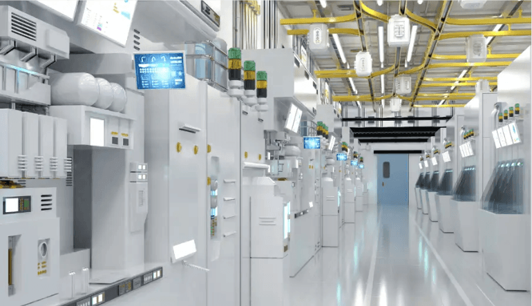
The global semiconductor industry is currently navigating an era of unprecedented complexity. As manufacturers push toward 3nm and 2nm process nodes, the focus of innovation has historically remained within the walls of the "fab"—on the lithography and etching processes that define modern computing power. However, as chips become more powerful, they also become significantly more fragile.
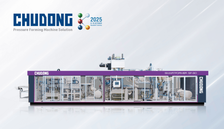
Discover CHUDONG SF-90 Thermoforming Innovation for Sustainable Food Packaging at K 2025
Step into any supermarket, café, or take-out restaurant, and you’ll find them everywhere—food trays stacked neatly, coffee cu p lids snapped on with a satisfying click, and takeaway boxes designed to hold your meal without a spill. These items feel so ordinary that most of us never pause to ask: Where do they come from? Behind these everyday products lies an invisible stage of innovation.